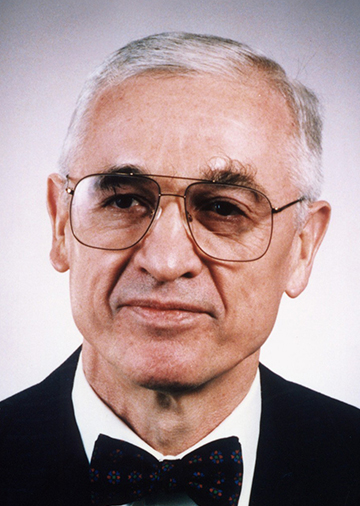
Professor, Center for Advanced Study, John Bardeen Chair Professor, University of Illinois
Dr. Holonyak was born in Illinois in the United States. He attended the University of Illinois and received his master of Science in 1951, and Ph. D. in Electrical Engineering in 1954. He was employed as a member of the technical staff at Bell Telefphone Laboratories and he helped to demonstrate the feasibility of the first diffused-impurity silicon devices, including transistors and oxide-masked transistors. In 1957, he joined the Advanced Semiconductor Laboratory of the General Electric Company, where he made great contributions in the areas of power and signal p-n-p-n devices, including his invention of the silicon controlled Rectifier (SCR).
These devices are now widely used in many places ranging homes to TV studios. From 1959, he focused his research on intermetallic compound semiconductors, and he elucidated new physical principles in the electronic processes involved.
He also tried unique methods in process technology for crystal growth and p-n junction formation. His work from 1960 to 1962 on GaAsP and his first construction of a p-n junction in this crystal system led to the commercial introdution of GaAsP light emitting diodes (LED).
He is the inventor of the first practical LED. In 1962 he succeeded in getting laser action in GaAsP.
This was the first visible light semiconductor laser. In 1963, he returned the University of Illinois as a professor. There he started an ambitious new research program on compound semiconductors. He accepted the challenge of developing ternary and quaternary intermetallic compound semiconductors, such as InGaP, InGaPAs, AlGaAsP etc., both for deeper understanding of physical principles and for practical applications.
He was the first to succeed in independently controlling two conditions lattice constant and energy gap. This achievement was a key contribution to the growth of modern optoelectronics. His research since 1976 has been characterized by his idea of the quantum-well structure.
He was the first to achieve continuous room temperature lasing by this structure in 1978. The concept of quantum-well structure formed the basis for novel quantum devices as well as modern optoelectronics.
As I have described, Dr. Holonyak's achievements ranging from research to practical developments on light-emitting diodes and semiconductor lasers through ambitious challenges in process technology of intermetallic compound semiconductors have been truly outstanding and creative, and gave tremendous stimules and enrichment to related fields of science and technology. Thus, Dr. Nick Holonyak, Jr. is a meritorious recipient deserving the 1995 (11th) Japan Prize.